Hello everyone, I believe that many netizens do not understand the ICT test principle and implementation, including the test principle of Youxin - ICT. However, it does not matter. Next, I will share with you some knowledge points about the ICT test principle and implementation and the test principle of Youxin - ICT. You can pay attention to the collection, so as not to find it next time. Let's start!
ICT test principle, ICT test parallel capacitor, how to test? Ask for the principle process
ICT online test principle
Abstract: This article introduces the basic knowledge and basic principles of online testing.
Online testing, ICT, In-Circuit Test, is a standard test method to check manufacturing defects and component defects by testing the electrical performance and electrical connections of online components. It mainly checks the open and short circuit conditions of individual components and various circuit networks on the line, and has the characteristics of simple operation, fast and rapid, and accurate fault location.
Flying probe ICT basically only performs static testing, and the advantage is that it does not require the production of fixtures and the program development time is short.
The needle bed ICT can perform analog device function and digital device logic function tests with high fault coverage, but a dedicated needle bed fixture must be made for each single board, and the fixture production and program development cycle is long.
Check the electrical performance of online components on the manufactured board and the connection of the circuit network. It can quantitatively measure components such as resistors, capacitors, inductors, crystal oscillators, perform functional tests on diodes, triodes, optocouplers, transformers, relays, operational amplifiers, power modules, etc., and perform functional tests on small and medium-sized integrated circuits, such as all 74 series, memory types, commonly used driver types, switching types, etc. IC.
It detects manufacturing process defects and component defects by directly testing the electrical performance of online devices. Component types can check out component value tolerance, failure or damage, memory type program errors, etc. For process types, faults such as solder short circuit, component mis-insertion, reverse insertion, missing installation, pin lift, cold soldering, PCB short circuit, broken wire, etc. can be found.
The fault of the test is directly located on the specific components, device pins, and network points, and the fault location is accurate. Repairing the fault does not require much professional knowledge. The program-controlled automated test is simple to operate and the test is fast and rapid. The test time of a single board is generally from a few seconds to tens of seconds.
Online testing is usually the first test process in production, which can timely reflect the production and manufacturing status and is conducive to process improvement and improvement. The faulty board tested by ICT can greatly improve production efficiency and reduce maintenance costs because of its accurate fault location and convenient repair. Because of its specific test project, it is one of the important test methods for modern mass production quality assurance.
Use operational amplifiers for testing. The concept of "virtual ground" from point "A" is:
Vs and Rref are the excitation signal source and instrument calculation resistance respectively. If V0 is measured, Rx can be obtained.
If the Rx to be tested is a capacitor or inductor, Vs is the AC signal source and Rx is in the form of impedance, and C or L can also be obtained.
The above test method is for independent devices, while the devices in the actual circuit are interconnected and affect each other, making Ix ref, and must be isolated (Guarding) during testing. Isolation is the basic technology of online testing.
In the above circuit, due to the shunting of the connection between R1 and R2, Ix ref, Rx = Vs/ V0*Rref does not hold. During the test, as long as G and F points are at the same potential, no current flows through R2, and Ix = Iref, Rx remains unchanged. Grounding point G, because point F is virtual ground, the potential of the two points is equal, then isolation can be achieved. In actual practice, G and F are made to have the same potential through an isolation operational amplifier. ICT testers can provide many isolation points to eliminate the influence of peripheral circuits on the test.
For digital ICs, Vector testing is used. Vector testing is similar to truth table measurement, stimulating input vectors, measuring output vectors, and judging the quality of devices through actual logic function tests.
For the test of analog IC, the voltage and current can be stimulated according to the actual function of IC, and the corresponding output can be measured as a functional block test.
With the development of modern manufacturing technology and the use of ultra-large-scale integrated circuits, it often takes a lot of time to write vector test programs for devices. For example, the test program of 80386 takes a skilled programmer nearly half a year. The large-scale application of SMT devices makes the fault phenomenon of device pin open circuit more prominent. For this reason, various companies have introduced non-vector test technology, Teradyne launched MultiScan; GenRad launched Xpress non-vector test technology.
DeltaScan uses the electrostatic discharge protection or parasitic diodes that almost all digital device pins and most mixed signal device pins have to perform simple DC current tests on independent pin pairs of the device under test. When the power supply of a board is cut off, the equivalent circuit of any two pins on the device is shown in the figure below.
1 Add a negative voltage to the ground on pin A, and the current Ia flows through the forward biased diode of pin A. Measure the current Ia flowing through pin A.
2 Maintain the voltage at pin A and add a higher negative voltage to pin B. Current Ib flows through the forward biased diode at pin B. Current Ia decreases due to current sharing in the common substrate resistance from pin A and pin B to ground.
3 Measure the current Ia flowing through pin A again. If Ia does not change (delta) when voltage is applied to pin B, there must be a wiring problem.
DeltaScan software combines test results from many possible pin pairs on the device to obtain accurate fault diagnosis. Signal pins, power and ground pins, and substrates are all involved in DeltaScan testing, which means that in addition to pin disconnection, DeltaScan can also detect manufacturing faults such as missing components, reverse insertion, and disconnected wires.
GenRad-type testing is called Junction Xpress. It also uses the diode characteristics in the IC, but the test is achieved by measuring the spectrum characteristics (second harmonics) of the diode.
DeltaScan technology does not require additional fixture hardware, making it the first choice.
FrameScan uses capacitive coupling to detect pin disconnection. Each device has a capacitive probe on it. When a signal is stimulated on a pin, the capacitive probe picks up the signal. As shown in the figure:
1 The multi-way switch board on the fixture selects the capacitive probe on a device.
2 The analog test board (ATB) in the tester sends an AC signal to each pin under test in turn.
3 The capacitive probe collects and buffers the AC signal on the pin under test.
4 The ATB measures the AC signal picked up by the capacitive probe. If the connection between a pin and the circuit board is correct, a signal will be measured; if the pin is disconnected, there will be no signal.
GenRad-like technology is called Open Xpress. The principle is similar.
This technology requires sensors and other hardware for the fixture, and the test cost is slightly higher.
ICT testers require at least one test point for each circuit node. However, with the increasing integration of devices, more powerful functions, smaller packages, more SMT components, the use of multilayer boards, and the increase in component density on PCB boards, it becomes very difficult to place a probe at each node. In order to increase the number of test points, the manufacturing cost increases; at the same time, it becomes difficult to develop a test library for a powerful device, and the development cycle is extended. For this reason, the Joint Test Association (JTAG) promulgated the IEEE1149.1 test standard.
IEEE1149.1 defines several important characteristics of a scanning device. First, the four (five) pins that make up the test access port (TAP) are defined: TDI, TDO, TCK, TMS, (TRST). The test mode selection (TMS) is used to load control information; secondly, several different test modes supported by the TAP controller are defined, mainly external test (EXTEST), internal test (INTEST), and execution test (RUNTEST); finally, the boundary scan language (Boundary Scan Description Language) is proposed. BSDL language describes important information of scanning devices. It defines pins as input, output and bidirectional types, and defines TAP modes and instruction sets.
Each pin of a device with boundary scan is connected to a sequence shift register (SSR) unit, called a scan unit. The scan units are connected together to form a shift register chain, which is used to control and detect device pins. Its specific four pins are used to complete the test task.
Connecting the scan chains of multiple scanning devices together through their TAPs forms a continuous boundary register chain. Adding a TAP signal at the head of the chain can control and detect the pins of all devices connected to the chain. Such virtual contact replaces the physical contact of the bed of nails fixture on each pin of the device. Contact, virtual access replaces actual physical access, removes a large number of test pads that occupy PCB board space, and reduces the manufacturing cost of PCB and fixtures.
As a test strategy, when designing for testability of PCB boards, special software can be used to analyze circuit points and devices with scanning functions to determine how to effectively place a limited number of test points without reducing test coverage, and to reduce test points and test needles in the most economical way.
Boundary scan technology solves the difficulty of not being able to increase test points. More importantly, it provides a simple and quick way to generate test patterns. Software tools can be used to convert BSDL files into test patterns, such as Teradyne's Victory, GenRad's Basic Scan and Scan Path Finder. Solve the difficulty of writing complex test libraries.
TAP access port can also be used to realize online programming (In-System Program or On Board Program) for CPLD, FPGA, Flash Memroy.
Nand-Tree is a testability design technology invented by Inter. In our products, only this design is found in 82371 chip. There is a general program *.TR2 file describing its design structure, which we can convert into test vectors.
ICT testing must achieve accurate fault location and stable testing, which is closely related to circuit and PCB design. In principle, we require that each circuit network point has a test point. Circuit design must be isolated from the status of each device and cannot affect each other. Boundary scan and Nand-Tree design must be installed with testability requirements.
MOS tubes can generally only measure one-step diode conduction, and general ICT tests often falsely test
1. Generally, the D S pole tests its diode voltage
2. Another method is to use three-point testing, with the two pole needles of D S at A B, The G pole needle point number is at the isolation point 1, using the N mode, the standard value is 0.2V, the control pole voltage is adjusted between 2-5V, the lower limit can be enlarged to about 80%, and the upper limit is about 15%, depending on the actual situation
3. The above method is used for N-channel enhancement MOS tubes
ICT, In-Circuit Test, is a standard test method for checking manufacturing defects and component defects by testing the electrical performance and electrical connections of online components. It mainly checks the open and short circuit conditions of each circuit network on the line, and has the characteristics of simple operation, fast and rapid, and accurate fault location.
ICT is a combination of the three English words Information, Communication and Technology (Information and Communications Technology, referred to as ICT). It is a new concept and new technical field formed by the integration of information technology and communication technology.
At the beginning of the 21st century, the Group of Eight published the Okinawa Charter for the Global Information Society in Okinawa, stating that "information and communication technology is one of the most powerful driving forces for social development in the 21st century and will quickly become an important driving force for world economic growth."
In fact, the information and communication industry has different understandings of ICT. As a technology, the general understanding is that ICT can not only provide a variety of services based on broadband and high-speed communication networks, but also transmit and share information, and is also a universal smart tool. As for how many services there will be and how "smart" this tool will be, the current concept is still very vague. The integration of the three networks is only a foundation and prelude to ICT, and IPTV, mobile TV, etc. are probably just the tip of the iceberg.
For fixed-line operators that have already sounded the horn of transformation, ICT is currently more of a service provided to customers. This service is a combination and integration of IT (information industry) and CT (communication industry). The communication industry, electronic information industry, Internet, and media industry will all be integrated within the scope of ICT. Fixed-line operators such as China Telecom provide customers with one-stop ICT services, including integration services, outsourcing services, professional services, knowledge services and software development services. In fact, ICT services not only provide enterprise customers with solutions for line construction and network architecture, but also reduce the burden of enterprises in establishing applications, system upgrades, operation and maintenance, security, etc., saving enterprise operating costs, and are therefore welcomed by enterprise users.
In China Telecom's corporate strategic transformation guidelines, ICT has become one of the four major business expansion areas alongside Internet applications, video content and mobile communications. The background of ICT is the integration of industries and the strong demand for information and communication services. The entry of fixed-line operators into the ICT field is a choice made when fixed-line space is squeezed everywhere and enterprises are tired of development or even in a recession. Strictly speaking, it is a crisis transformation or a weak transformation. Among the pioneers of transformation, there are companies such as Nokia that have successfully transformed from the wood processing industry to the IT industry, and there are also century-old companies such as AT&T that ended sadly during the transformation process. Therefore, it is necessary for China's fixed-line operators to comprehensively examine the distance between themselves and IT companies. Let's make a simple comparison between IT companies and CT companies.
CT and IT both belong to the information industry, with similar industrial characteristics. There are many overlapping nodes in the industrial chain, which complement each other and are inseparable. On the one hand, many IT manufacturers are also CT equipment suppliers, such as equipment manufacturers that produce network switches and routers. On the other hand, CT itself is the main customer of the IT service industry. For example, in 2004, the telecommunications industry accounted for 17.9% of the industry structure of China's IT service market, ranking second only to the financial industry (18.6%). At the same time, in the informationization process, the integration of IT and CT is becoming closer and closer. Usually, a successful information application system must organically combine the knowledge and resources of both IT and CT to achieve success, such as remote education, remote medical care, e-agriculture, e-government, e-commerce, information security and other fields.
1. Different capital structures. The industry characteristics of CT are capital-intensive fields. It is difficult to enter without certain strength. It has economies of scale. Equipment and capital are the main production factors. The IT service industry is an intellectual-intensive field, and people are the main production factors of enterprises. IBM's IT service operating income accounts for about 40% of the entire business. At the same time, 130,000 service professionals around the world account for half of IBM's total employees. For IT service providers, personnel investment is the main investment. Take a service contract signed by IBM in 2003 with Swiss power and automation technology company ABB as an example. The service contract will generate US$1.7 billion in revenue in 10 years, but IBM will pay more than US$90 million in labor costs each year for this. In total, the labor cost ratio is 53%.
2. Different content provided. CT services mainly provide functional product services, such as telephone, broadband access, PHS, networking, etc., with some value-added services; IT services are mainly human services, relying on technical services and providing solutions to make profits.
3. Different product life cycles. CT products have a long life cycle. It has been more than a hundred years since Bell invented the telephone in 1876, and broadband is still in its growth stage after so many years. IT services require high-tech support, the evolution of technology is very closely related, and the product life cycle is short.
4. Different employment characteristics. CT companies have formed a complete employment system for a long time. The salary, job system, and career development of employees have a relatively fixed model, and the workforce is relatively stable; the IT industry has a concentration of knowledge-based employees, a flexible employment system, and a large employee mobility. According to the survey, nearly 40% of IT company employees are ready to change jobs at any time due to salary, work pressure, career development, etc.
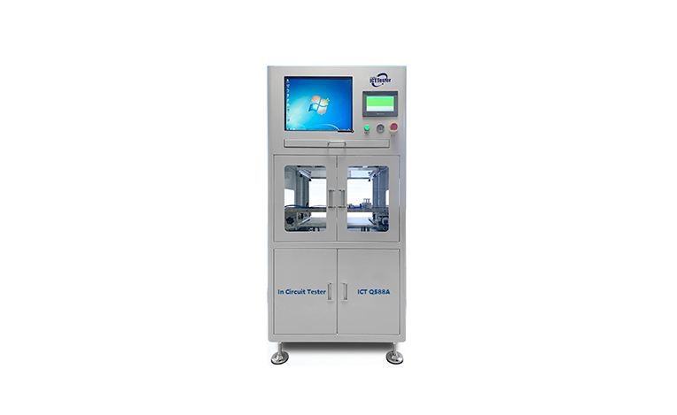
In-Circuit-Tester, referred to as ICT, is an automatic online tester. It is a test device for PCBA (Printed- Circuit Board Assembly) production that is essential for modern electronic companies. ICT has a wide range of uses, high measurement accuracy, and clear indications for detected problems. Even workers with average electronic technology levels can easily handle problematic PCBAs. The use of ICT can greatly improve production efficiency and reduce production costs. 2. ICT Test mainly uses the test probe to contact the test points on the PCB layout to detect the open circuit, short circuit, and welding status of all parts of the PCBA. It can be divided into open circuit test, short circuit test, resistance test, capacitance test, diode test, transistor test, field effect transistor test, IC pin test (testjet` connect check) and other common and special components missing, wrong installation, input value deviation, solder joint welding, circuit board open and short circuit and other faults, and accurately tell the user which component or open and short circuit is the fault. (It has a high recognition ability for component welding test) 3. ICT devices are manufactured by different manufacturers. ICT produced by TRI, OKANO, JET, TESCON, POSSEHL, SAMSUNG (FARA), CONCORD, GW, TAKAYA, SYSTEM, SRC, etc. are all used in China.
According to the mechanical dimension drawing of the circuit board, the DIP pins and test points on the circuit board are punched, and then the pins are inserted.
The network (NET) in the circuit board is the PCB trace, and all are led out. The purpose of using instruments to test whether the internal circuit structure is OK is achieved.
As an important analytical method, the spectral analysis method plays a great role in scientific research, production, quality control, etc. Whether it is penetrating absorption spectroscopy, fluorescence spectroscopy, or Raman spectroscopy, obtaining single-wavelength radiation is an indispensable means. Since modern monochromators can have a wide spectral range (UV-IR), high spectral resolution (0.001nm), automatic wavelength scanning, complete computer control functions, and are very easy to cooperate with other peripheral devices to form a high-performance automatic test system, the use of computer automatic scanning multi-grating spectrometers has become the first choice for spectral research.
In spectroscopy applications, obtaining single-wavelength radiation is an indispensable means. In addition to using monochromatic light sources (such as spectrum lamps, lasers, light-emitting diodes), color glass and interference filters, most of them use scanning wavelength selection monochromators. In particular, scanning grating monochromators are more commonly used to select narrow spectrum (monochromatic or single wavelength) radiation in a continuous wide wavelength range (white light).
When a beam of composite light enters the incident slit of the spectrometer, it is first collimated into parallel light by an optical collimator, and then dispersed into separate wavelengths (colors) by a diffraction grating. Using the different angles at which different wavelengths leave the grating, the focusing reflector is used to image the exit slit. The exit wavelength can be precisely changed through computer control.
As an important spectroscopic device, the selection and performance of the grating directly affect the performance of the entire system. To better assist users in their selection, a brief introduction is given here.
Gratings are divided into ruled gratings, replica gratings, holographic gratings, etc. Ruled gratings are mechanically scratched on a metal-coated surface with a diamond cutter; replica gratings are copied from a master grating. The grooves of typical ruled gratings and replica gratings are triangular. Holographic gratings are made by laser interference fringe lithography. Holograms usually include sinusoidal grooves. Ruled gratings have the characteristics of high diffraction efficiency, a wide spectral range, low stray light, and high spectral resolution.
Reflective diffraction gratings are periodically scratched on a substrate with many fine grooves. The intervals between a series of parallel grooves are equivalent to the wavelength, and a layer of high reflectivity metal film is coated on the grating surface. The interaction of radiation reflected from the grating groove surface produces diffraction and interference. For a certain wavelength, it disappears in most directions and only appears in certain limited directions. These directions determine the diffraction order. As shown in Figure 1, the grating groove is perpendicular to the radiation incident plane, the incident angle between the radiation and the grating normal is α, the diffraction angle is β, the diffraction order is m, and d is the groove spacing. The maximum value of interference is obtained under the following conditions:
Define φ as half of the angle between the incident light and the diffracted light, that is, φ=(α-β)/2; θ is the grating angle relative to the zero-order spectral position, that is, θ=(α+β)/2, and a more convenient grating equation is obtained:
For a given direction β, there can be several wavelengths corresponding to the order m λ that satisfy the grating equation. For example, the first-order radiation of 600nm, the second-order radiation of 300nm, and the third-order radiation of 200nm have the same diffraction angle.
Multiple wavelengths of the same order are distributed at different β.
The radiation direction containing multiple wavelengths is fixed, the grating is rotated, and α is changed, then different wavelengths are obtained in the direction where α+β remains unchanged.
The groove density G=1/d, d is the groove spacing, and the unit is mm.
The blaze wavelength is the point of maximum diffraction efficiency of the grating. Therefore, when selecting a grating, the blaze wavelength should be selected as close to the actual required wavelength as possible. If the actual application is in the visible light range, the blaze wavelength can be selected as 500nm.
The number of grating lines is directly related to the spectral resolution. More lines have high spectral resolution, and fewer lines have wide spectral coverage. Both should be flexibly selected according to the experiment.
The grating efficiency is the ratio of monochromatic light diffracted to a given order to the incident monochromatic light. The higher the grating efficiency, the smaller the signal loss. In order to improve this efficiency, in addition to improving the grating manufacturing process, special coatings are also used to improve the reflection efficiency.
The resolution R of the grating spectrometer is a measure of the ability to separate two adjacent spectral lines. According to the Rayleigh criterion:
The practical definition of the grating spectrometer is to measure the half-height width (FWHM) of a single spectral line. In fact, the resolution depends on the resolving power of the grating, the effective focal length of the system, the set slit width, the optical aberration of the system, and other parameters.
M--number of grating lines F--focal length of spectrometer W--slit width
The dispersion of the grating spectrometer determines its ability to separate wavelengths. The reciprocal dispersion of the spectrometer can be calculated: the change in wavelength λ caused by changing the distance χ along the focal plane of the monochromator, that is:
Here d, β, and F are the spacing of the grating grooves, the diffraction angle, and the effective focal length of the system, respectively, and n is the diffraction order. As can be seen from the equation, the reciprocal dispersion is not a constant, it changes with wavelength. Within the wavelength range used, the change may exceed 2 times. According to national standards, in this sample, the reciprocal dispersion at the middle value of the 1200l/mm grating dispersion (typically 435.8nm) is used.
Bandwidth is the wavelength width output from the spectrometer at a given wavelength, ignoring optical aberrations, diffraction, scanning methods, detector pixel width, slit height, and illumination uniformity. It is the product of the reciprocal dispersion and the slit width. For example, if the monochromator slit is 0.2mm and the grating inverse linear dispersion is 2.7nm/mm, the bandwidth is 2.7*0.2=0.54nm.
Wavelength accuracy is the scale level of the spectrometer to determine the wavelength, and the unit is nm. Usually, wavelength accuracy varies with wavelength, and this sample is the worst case.
Wavelength repeatability is the ability of the spectrometer to set a wavelength, change the setting, and then return to the original wavelength. This reflects the stability of the wavelength drive mechanism and the entire instrument. Zhuoli Hanguan's spectrometer has excellent wavelength drive and mechanical stability, and its repeatability exceeds wavelength accuracy.
Wavelength accuracy is the difference between the spectrometer's set wavelength and the actual wavelength. Each monochromator must check wavelength accuracy at many wavelengths.
F/# is defined as the ratio of the spectrometer's diameter to the focal length. This is a measure of the spectrometer's acceptance angle, which is an important parameter for adjusting the coupling of the monochromator to the light source and detector. When F/# is matched, the full aperture of the spectrometer can be used. However, most monochromators use rectangular optical components. Here F/# is defined as the ratio of the equivalent diameter of the spectrometer to the focal length. The equivalent diameter of a rectangular optical component is the diameter of a circle with the same area.
LCR tester is used to measure the inductance of a coil, the capacitance of a capacitor, and the resistance of a resistor. It is a measuring instrument made using the bridge principle and can perform relatively accurate measurements. For detailed information, please go to Ritu to inquire. It specializes in instrumentation.
Main features of ED2671A universal AC/DC withstand voltage tester
◆ It is designed in accordance with domestic and international safety standards such as IEC, ISO, BS, UL, and JIS, and can generate AC test high voltage and DC test high voltage.
◆ In addition to being suitable for safety testing of inductive electrical appliances, it can also be used to perform safety testing of capacitive household appliances and low-voltage electrical appliances. One machine has two uses.
◆ The test voltage and leakage current are displayed using a 4-digit LED digital tube, and the test time is displayed using a 2-digit LED digital tube.
◆ The leakage current value is adjusted by the coarse and fine adjustment knobs.
◆When the leakage current exceeds the tolerance, the test voltage is automatically cut off and an audible and visual alarm signal is issued.
Main technical parameters of ED2671A universal AC/DC withstand voltage tester
◆Test voltage: AC/DC 0~10KV (ED2677)
◆Leakage current range: AC 0.01mA~20mA DC 0.01mA~10mA
END, this article ends here. If it can help you, please pay attention to this site!